St Petersburg University scientists study the formation mechanisms of materials for a new generation of optoelectronic devices
Physicists from St Petersburg University and their colleagues from other research and educational organisations in St Petersburg have studied the formation of InGaN ternary compounds in the three-dimensional growth mode. InGaN ternary compounds are a promising semiconductor alloy of indium gallium nitride. The study will help to create a new generation of non-planar optoelectronic devices in the field of electronics and communications.
InGaN (indium gallium nitride) is a semiconductor material made of a mix of gallium and indium nitrides. White and blue LEDs are based on this material. InGaN is also promising for creating gas sensing applications, solar battery elements, cells for hydrogen synthesis, and red, green and white LEDs and others.
The research findings are published in ACS Applied Nano Materials
Currently, the material is not widely used because it is difficult to synthesise InGaN layers in a wide range of compositions due to the phenomenon of ‘solubility gap’. In other words, InGaN is unstable and disintegrates into separate InN and GaN phases. It is also difficult to integrate with a silicon platform due to the difference in the constant crystal lattices between these materials.
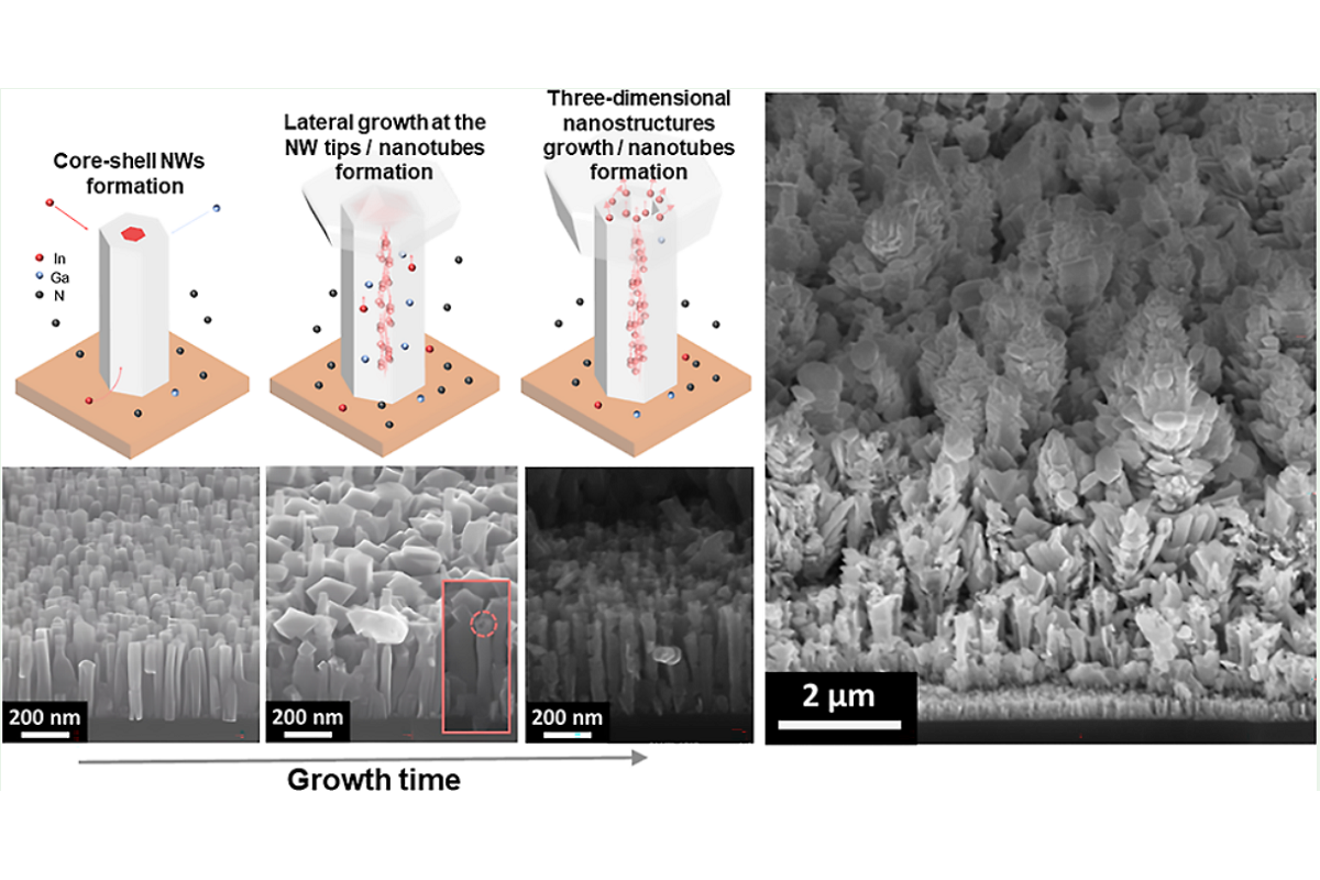
This problem can be solved by synthesising the material directly on the silicon surface in a complex form, i.e. core—shell nanowires (NWs), nanotubes, nanoflowers and other forms. This approach to synthesis also significantly expands the potential for using this material for different devices. Yet, according to the physicists, if we want to use this alloy in the most effective and complete way, we need to understand the mechanisms of formation of these complex three-dimensional nanostructures. The study of St Petersburg University scientists provides just such an emphasis. The study was carried out together with Alferov Saint Petersburg National Research Academic University, the Institute for Problems in Mechanical Engineering of the Russian Academy of Sciences, and the Higher School of Economics.
For the first time, we studied the complex mechanism of formation of three-dimensional (non-planar) structures based on InGaN material, using scientific and systematic approaches to describe the growth processes of this structure. Based on such compounds, prototypes of LEDs, gas sensors, water decomposition cells, etc. are already being created at the laboratory at St Petersburg University.
Rodion Reznik, Head of the Laboratory of New Semiconductor Materials for Quantum Informatics and Telecommunications at St Petersburg University
‘Gaining a deeper insight into the mechanisms of formation of these complex three-dimensional nanostructures can contribute to the creation of a new generation of non-planar optoelectronic devices,’ said Rodion Reznik, Head of the Laboratory of New Semiconductor Materials for Quantum Informatics and Telecommunications at St Petersburg University.
We can grow this compound by plasma-assisted molecular beam epitaxy, i.e. a method that allows growing heterostructures with specified properties in ultra-high vacuum conditions, said Rodion Reznik. The method allows creating effective new-generation devices.
The study was conducted using the state-of-the-art scientific equipment and infrastructure at the Laboratory of New Semiconductor Materials for Quantum Informatics and Telecommunications at St Petersburg University. The study also involved scientists from the Higher School of Economics, Alferov Saint Petersburg National Research Academic University, and the Institute for Problems in Mechanical Engineering of the Russian Academy of Sciences.
Members of the Laboratory of New Semiconductor Materials for Quantum Informatics and Telecommunications at St Petersburg University are studying new materials for microelectronics: sources of single photons, efficient LEDs, solar cells, lasers, and nanopiezoelectric generators to integrate them with a silicon platform. All these achievements are a continuation of the work on improving quantum technologies for microelectronics, laid down by two Nobel laureates: Alexey Ekimov, a graduate of St Petersburg University, Nobel laureate in chemistry; and Zhores Alferov, the founder and Rector of Alferov Saint Petersburg National Research Academic University. You can find more information in the Heinrich Terahertz podcast by St Petersburg University..
If we synthesise nitride compounds using a research setup, the synthesis process using molecular beam epitaxy is quite long. Yet, as a result, we get a large plate that can be cut into hundreds of small pieces, each of which is the basis for a device.
‘We have carried out systematic work on the synthesis of nanostructures and the study of their properties at various stages of growth. In other words, we synthesised a series of samples, where the growth of each of them stopped at a certain stage of the formation of nanostructures. Then, the physical properties of each sample were studied using unique equipment. The results of the research enabled us to gain an insight into the mechanisms of the formation of InGaN nanostructures of complex shape to determine the parameters for the theoretical description of the growth processes, which was also carried out as part of the work,’ said Vladislav Gridchin, Junior Research Associate in the Laboratory of New Semiconductor Materials for Quantum Informatics and Telecommunications at St Petersburg University and the main author of the article.
St Petersburg University, the oldest university in Russia, was founded on 28 January (8 February) 1724. This is the day when Peter the Great issued a decree establishing the University and the Russian Academy of Sciences. Today, St Petersburg University is an internationally recognised centre for education, research and culture. In 2024, St Petersburg University celebrates its 300th anniversary.
The plan of events during the celebration of the anniversary of the University was approved at the meeting of the Organising Committee for the celebration of St Petersburg University’s 300th anniversary. The meeting was chaired by Dmitry Chernyshenko, Deputy Prime Minister of the Russian Federation. Among the events are: the naming of a minor planet in honour of St Petersburg University; the issuance of bank cards with a special design; and the branding of the aircraft of the Rossiya Airlines to name just a few. To mark the 300th anniversary of St Petersburg University, a postage stamp depicting the Twelve Collegia building and the monument to Count Sergey Uvarov was issued. Also, a Soyuz rocket bearing the symbols of the University was launched from the Baikonur Cosmodrome.
By the decision of the Governor of St Petersburg Alexander Beglov, 2024 is a year of the 300th anniversary of St Petersburg University in St Petersburg. On the day of the University’s 300th anniversary torches were lit on the Rostral Columns on the Spit of Vasilyevsky Island. St Petersburg University flags were raised on the Palace Bridge. The city public transport was decorated with the University’s symbols. During St Petersburg’s City Day celebrations in May 2024, St Petersburg University acted as a participating venue. Additionally, the University has launched a website dedicated to the anniversary. The website contains information about outstanding University staff, students, and alumni; scientific achievements; and details of events held as part of the celebration of the 300th anniversary of the University.